
DEPARTMENT INSTRUMENTATION
JEOL – JEM 1400. 120 keV accelerating voltage; electron gun assembly with cool beam illumination system - LaB6 filament. Point resolution: 0.38 nm; Lattice resolution: 0.20 nm; Accelerating voltage range: 40, 60, 80, 100, 120 keV; equipped with energy dispersive spectroscopy.
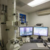
The Department of Engineering also has a FEI Quanta 450FEG SEM at the Nano Instrumentation Center.
One of the most comprehensive Scanning Electron Microscopes, the FEI Quanta 450FEG SEM, equipped with the latest Energy Dispersive Spectrometer (Oxford Aztec Energy Advanced EDS System) is housed in the College of Engineering. These Nanotechnology tools address the need to investigate a wide variety of materials and characterize structure and composition. The lab aims to enhance the education, collaboration, research, and outreach related to all aspects of electron probe instrumentation, techniques and applications. The facility is multi-user and cross-departmental—open to any qualified scientist to use, with our qualified microscopist and material scientist Dmitriy Dikin offering training and technical support.
KEY FEATURES:
- High resolution FEG-SEM with ESEM technology
- SE and BSE imaging in every mode of operation allowing for characterization of conductive and non-conductive samples
- Low vacuum and ESEM capability enables charge-free imaging and analysis of non-conductive and/or hydrated specimens allowing for minimized sample preparation
- Capable of EDS analysis on conductive and non-conductive samples in high and low vacuum
- Imaging with beam deceleration mode to get surface and compositional information from conductive samples
- Easy to use, intuitive software makes highly effective operation possible for novice users
- Possible additions: Perform dynamic in situ analysis of samples in their natural state above or below ambient temperatures from - 165 °C to 1000 °C with specialized in situ stages. High resolution bright and dark field imaging of thin slices of materials by scanning transmission electron detector (STEM). In situ mechanical and electrical measurements.